- 您现在的位置:买卖IC网 > Sheet目录3882 > PIC18F4539T-I/ML (Microchip Technology)IC MCU FLASH 12KX16 EE A/D 44QFN
PIC18FXX39
DS30485A-page 146
Preliminary
2002 Microchip Technology Inc.
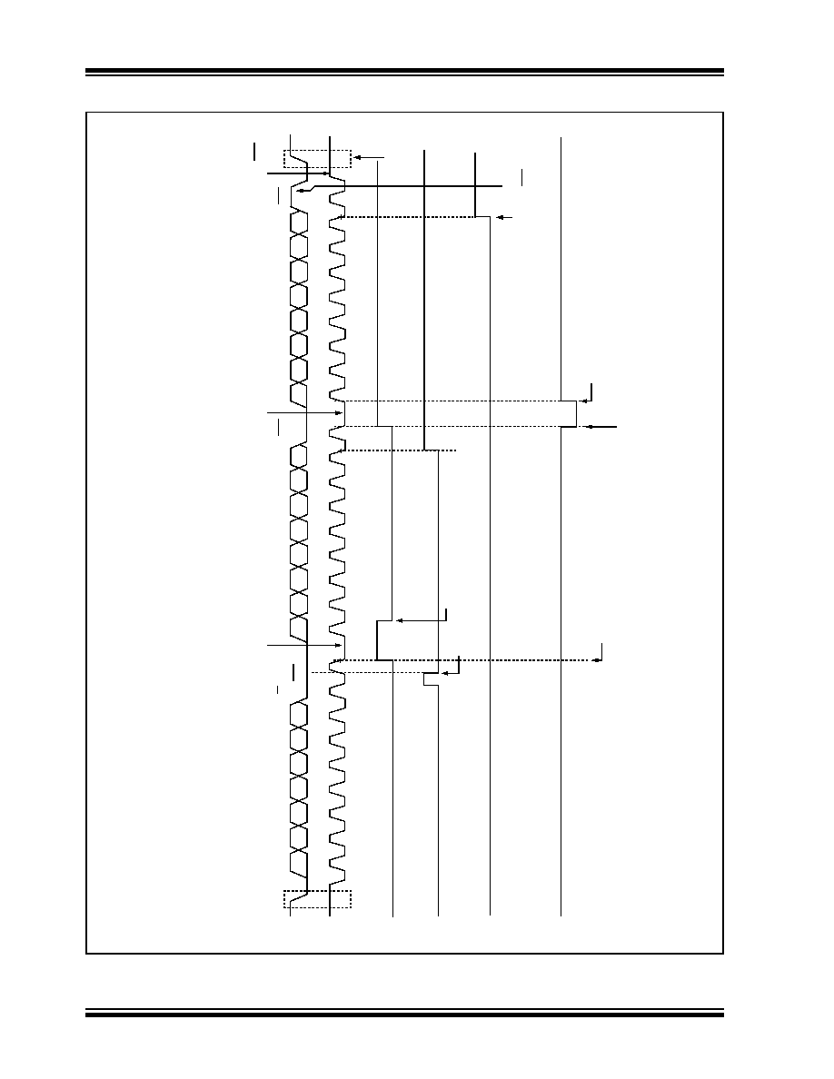
FIGURE 16-13:
I2C SLAVE MODE TIMING WITH SEN = 1 (RECEPTION, 7-BIT ADDRESS)
SDA
SCL
SS
PI
F
BF
(
S
SPS
TA
T
<
0
>
)
SSP
O
V
(
S
SPCO
N
<
6>
)
S
1
2
3
4
56
7
8
9
1
23
4
5
6
7
89
1
2
3
4
5
7
8
9
P
A
7
A6
A
5
A4
A
3
A2
A
1
D7
D6
D5
D4
D3
D
2
D1
D0
D7
D6
D5
D4
D3
D1
D0
ACK
Re
ce
ivin
gDa
ta
ACK
Re
ce
ivin
gDa
ta
R/W
=
0
ACK
R
e
cei
vi
ng
A
ddr
ess
Cle
a
re
d
in
so
ftwa
re
SSP
BUF
is
re
a
d
B
u
sM
a
st
er
ter
m
inate
s
tra
n
sfer
S
SPO
V
is
se
t
b
e
ca
us
e
SS
PBU
F
is
still
fu
ll.
ACK
is
n
o
tsent
.
D2
6
(P
IR
1<
3>
)
CK
P
CK
P
wr
itte
n
to
‘1
’in
If
B
F
is
cleare
d
pr
ior
to
the
fa
llin
g
edg
e
of
the
9th
cl
ock,
CKP
will
n
ot
b
e
r
e
se
t
to
‘0
’and
n
o
clock
str
e
tch
in
g
will
o
ccu
r
softwar
e
Clo
ck
is
h
e
ld
lo
w
u
n
til
CK
P
is
set
to
‘1’
Clo
ck
is
n
o
th
e
ld
lo
w
be
cause
b
u
ffer
ful
lbi
ti
s
cl
ear
pr
io
rto
fal
ling
ed
ge
of
9th
cl
ock
Clo
ck
is
n
o
th
e
ld
lo
w
becau
se
A
C
K
=
1
BF
is
se
ta
fte
r
fa
llin
g
edge
o
fthe
9
th
cl
ock,
CKP
is
r
e
se
tto
‘0
’a
nd
clock
str
e
tch
ing
occu
rs
发布紧急采购,3分钟左右您将得到回复。
相关PDF资料
PIC18LF2539T-I/SO
IC MCU FLASH 12KX16 EE AD 28SOIC
PIC18LF4539T-I/PT
IC MCU FLASH 12KX16 EE AD 44TQFP
PIC16LF874AT-I/ML
IC MCU FLASH 4KX14 A/D 44QFN
PIC16F77T-E/ML
IC MCU FLASH 8KX14 A/D 44QFN
PIC16F874A-E/ML
IC MCU FLASH 4KX14 A/D 44QFN
PIC16F74T-I/ML
IC MCU FLASH 4KX14 A/D 44QFN
PIC16F77T-I/ML
IC MCU FLASH 8KX14 A/D 44QFN
PIC18F24K20-I/SS
IC PIC MCU FLASH 8KX16 28SSOP
相关代理商/技术参数
PIC18F4539T-I/PT
功能描述:8位微控制器 -MCU 24KB 1408 RAM 32 I/O RoHS:否 制造商:Silicon Labs 核心:8051 处理器系列:C8051F39x 数据总线宽度:8 bit 最大时钟频率:50 MHz 程序存储器大小:16 KB 数据 RAM 大小:1 KB 片上 ADC:Yes 工作电源电压:1.8 V to 3.6 V 工作温度范围:- 40 C to + 105 C 封装 / 箱体:QFN-20 安装风格:SMD/SMT
PIC18F4550EPT
制造商:Microchip Technology Inc 功能描述:
PIC18F4550-I/ML
功能描述:8位微控制器 -MCU 32kBF 2048RM FSUSB2 RoHS:否 制造商:Silicon Labs 核心:8051 处理器系列:C8051F39x 数据总线宽度:8 bit 最大时钟频率:50 MHz 程序存储器大小:16 KB 数据 RAM 大小:1 KB 片上 ADC:Yes 工作电源电压:1.8 V to 3.6 V 工作温度范围:- 40 C to + 105 C 封装 / 箱体:QFN-20 安装风格:SMD/SMT
PIC18F4550-I/P
功能描述:8位微控制器 -MCU 32kBF 2048RM FSUSB2 RoHS:否 制造商:Silicon Labs 核心:8051 处理器系列:C8051F39x 数据总线宽度:8 bit 最大时钟频率:50 MHz 程序存储器大小:16 KB 数据 RAM 大小:1 KB 片上 ADC:Yes 工作电源电压:1.8 V to 3.6 V 工作温度范围:- 40 C to + 105 C 封装 / 箱体:QFN-20 安装风格:SMD/SMT
PIC18F4550-I/PT
功能描述:8位微控制器 -MCU 32kBF 2048RM FSUSB2 RoHS:否 制造商:Silicon Labs 核心:8051 处理器系列:C8051F39x 数据总线宽度:8 bit 最大时钟频率:50 MHz 程序存储器大小:16 KB 数据 RAM 大小:1 KB 片上 ADC:Yes 工作电源电压:1.8 V to 3.6 V 工作温度范围:- 40 C to + 105 C 封装 / 箱体:QFN-20 安装风格:SMD/SMT
PIC18F4550T-I/ML
功能描述:8位微控制器 -MCU 32kBF 2048RM FSUSB2 RoHS:否 制造商:Silicon Labs 核心:8051 处理器系列:C8051F39x 数据总线宽度:8 bit 最大时钟频率:50 MHz 程序存储器大小:16 KB 数据 RAM 大小:1 KB 片上 ADC:Yes 工作电源电压:1.8 V to 3.6 V 工作温度范围:- 40 C to + 105 C 封装 / 箱体:QFN-20 安装风格:SMD/SMT
PIC18F4550T-I/PT
功能描述:8位微控制器 -MCU 32kBF 2048RM FSUSB2 RoHS:否 制造商:Silicon Labs 核心:8051 处理器系列:C8051F39x 数据总线宽度:8 bit 最大时钟频率:50 MHz 程序存储器大小:16 KB 数据 RAM 大小:1 KB 片上 ADC:Yes 工作电源电压:1.8 V to 3.6 V 工作温度范围:- 40 C to + 105 C 封装 / 箱体:QFN-20 安装风格:SMD/SMT
PIC18F4553-I/ML
功能描述:8位微控制器 -MCU 32KB FLSH 2048 RAM FSUSB 2.0 12B ADC RoHS:否 制造商:Silicon Labs 核心:8051 处理器系列:C8051F39x 数据总线宽度:8 bit 最大时钟频率:50 MHz 程序存储器大小:16 KB 数据 RAM 大小:1 KB 片上 ADC:Yes 工作电源电压:1.8 V to 3.6 V 工作温度范围:- 40 C to + 105 C 封装 / 箱体:QFN-20 安装风格:SMD/SMT